
 0
0



News & Events
Latest Updates & Industry Insights
- Home
- News
- Technical Knowledge
- High-End Semiconductor Handling Modules: ESD Engineering Plastics Selection Strategies and Practical Challenges
High-End Semiconductor Handling Modules: ESD Engineering Plastics Selection Strategies and Practical Challenges
May 05,2026
Technical Comparison and Practical Application of ESD PEEK, Semitron, and PTFE
In semiconductor cleanroom equipment, wafer handling modules must simultaneously meet three major requirements: high precision, low contamination, and electrostatic discharge (ESD) control. Among these, material selection directly impacts equipment stability, yield rate, and product reliability.A characteristics comparison and application analysis of three common ESD materials:
- ESD PEEK
- Semitron ESD Series (Semitron anti-static engineering plastics)
ESD Material Characteristics Comparison
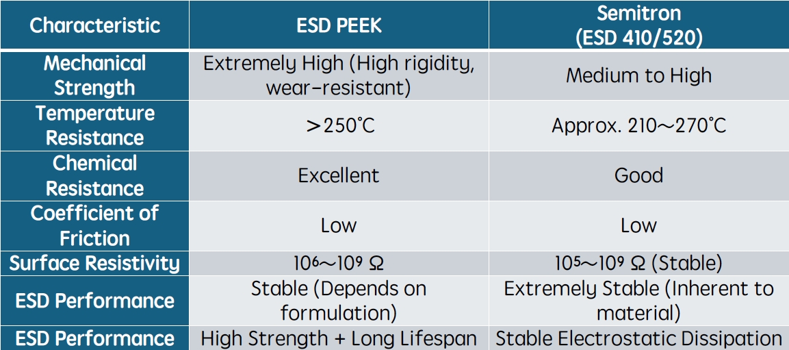
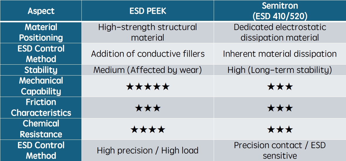
Material Application Differences Analysis
Selection Recommendatio
In the design of wafer handling modules, rapid assessments can be made based on requirements:- High rigidity / High precision / Long lifespan → Choose ESD PEEK
- Stable ESD control / Low Particle → Choose Semitron (ESD 410/520)
Key Design Considerations
Besides the inherent characteristics of the materials, the following must be noted in practice:- Process Environment Impact
Temperature cycling → Material thermal expansion; Humidity → Electrostatic impact; Chemical liquids → Material degradation
- ESD Coating Process Risks
When aluminum alloy (AL) structural components undergo the ESD coating process, baking temperatures and thermal cycling conditions must be strictly controlled.
Improper heat treatment can trigger the release of residual stress (Stress Relief) within the material, causing micro-deformation of the structure.
This will further affect the Robot's alignment precision (Alignment) and the repeatability of wafer picking and placing (Repeatability), resulting in a decline in overall handling stability.
- Mechanical Design Coordination
Grounding design; Contact area control (reducing triboelectric charging); Surface roughness (avoiding Particles)
Conclusion
In semiconductor wafer handling systems, there is no single best ESD material; rather, it is about optimal combinations based on application scenarios:- Structural Components → ESD PEEK
- Precision Contact Components → Semitron (ESD 410/520)
Common ESD-Related Failure Modes
- Wafer Attraction (Electrostatic Attraction)
→ Leads to pick-and-place failures - Mapping Misjudgment
→ Static electricity interferes with optical Sensors, causing errors in determining wafer presence - ESD Damage (Latent Damage)
→ Causes irreversible damage to advanced process chips - Particle Increase
→ Electrostatic attraction of micro-particles, affecting yield rate

